- 操作模式
|
MODE[1:0] |
Mode Selection |
OSR (fmod/fData) |
MAX fData |
|
00 |
High-Speed |
64 |
144531 |
|
01 |
High-Resolution |
128 |
52734 |
|
10 |
Low-Power |
64 |
52734 |
|
11 |
Low-Speed |
64 |
10547 |
MODE[1:0] |
Mode Selection |
MAX fCLK(MHz) |
CLKDIV |
fCLK/fData |
DATA RATE (SPS) |
|
00 |
High-Speed |
37 |
1 |
256 |
144531 |
|
01 |
High-Resolution |
27 |
1 |
512 |
52734 |
|
10 |
Low-Power |
27 |
1 |
512 |
52734 |
|
13.5 |
0 |
256 |
|||
|
11 |
Low-Speed |
27 |
1 |
2560 |
10547 |
|
5.4(5分频) |
0 |
512 |
NOTE: The SPI format is limited to a CLK input frequency of 27MHz, maximum. For CLK input operation above 27MHz (High-Speed mode only), use Frame-Sync format.
|
fCLK(MHz) |
VREF(V) |
DVDD |
Interface |
|
0.1<= fCLK<=27 |
0.5 to 3.1 |
1.65 to 1.95 |
Frams-Sync or SPI |
|
27<= fCLK<=32.768 |
0.5 to 2.6 |
1.65 to 1.95 |
Frams-Sync |
|
32.768<= fCLK<=37 |
0.5 to 2.1 |
2.0 to 2.2 |
Frams-Sync |
在High-Speed 模式下,若为TDM方式输出,因为8个Channel均通过OUT1输出且数据
为24bits,故必须保证 SCLK=clk
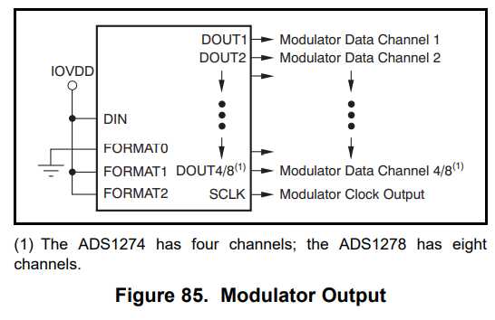
- Data Output Format
|
FORMAT[2:0] |
INTERFACE Protocol |
DOUT Mode |
Data Position |
|
000 |
SPI |
TDM |
Dynamic |
|
001 |
SPI |
TDM |
Fixed |
|
010 |
SPI |
Discrete |
– |
|
011 |
Frame-Sync |
TDM |
Dynamic |
|
100 |
Frame-Sync |
TDM |
Fixed |
|
101 |
Frame-Sync |
Discrete |
– |
|
110 |
Modulator Mode |
– |
– |
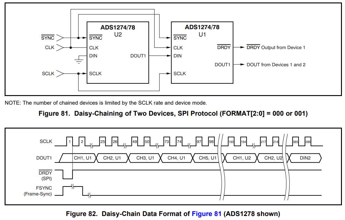
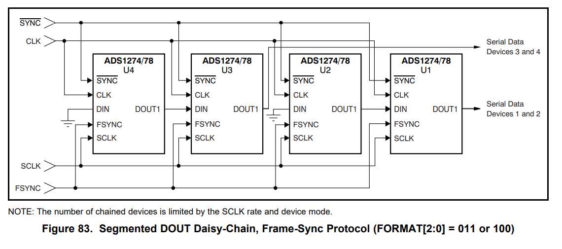
SPI/Frame-Sync:用相同的串行协议,使用相同的Pin
SCLK, DRDYn/FSYNC,DOUT[4:1](DOUT[8:1]),and DIN
The serial clock (SCLK) features a Schmitt-triggered input and shifts out data on DOUT on the falling edge. It also shifts in data on the falling edge on DIN when this pin is being used for daisy-chaining. The device shifts data out on the falling edge and the user normally shifts this data in on the rising edge
TDM mode(TDM Mode, Fixed-Position Data):
the data position of the channels remain fixed, regardless of whether the channels are powered down. If a channel is powered down, the data are forced to zero but occupy the same position within the data stream.
TDM Mode, Dynamic Position Data:
when a channel is powered down, the data from higher channels shift one position in the data stream to fill the vacated data slot. Figure 79 shows the data stream with channel 1 and channel 3 powered down
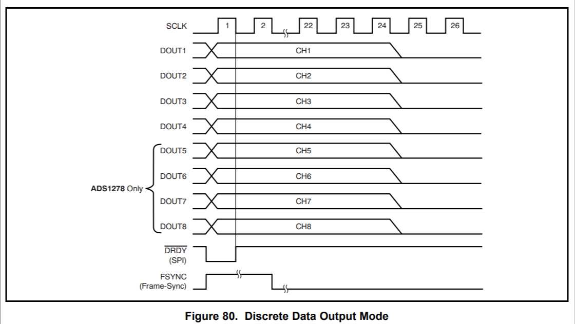
the channel data are shifted out in parallel using individual channel data output pins DOUT[4:1]/[8:1]. After the 24th SCLK, the channel data are forced to zero. The data are also forced to zero for powered down channels
- Daisy Chaining
MODE[1:0] |
Mode Selection |
CLKDIV |
Max Number of Channels |
|
00 |
High-Speed |
1 |
10 |
|
01 |
High-Resolution |
1 |
21 |
|
10 |
Low-Power |
1 |
21 |
|
0 |
10 |
||
|
11 |
Low-Speed |
1 |
106 |
|
0 |
21 |
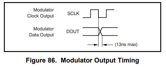
- Modulator Output clock Frequencies
(Format=110)
|
MODE[1:0] |
Mode Selection |
CLKDIV |
MODULATOR Clock Ouput (SCLK) |
|
00 |
High-Speed |
1 |
fCLK/4 |
|
01 |
High-Resolution |
1 |
fCLK/4 |
|
10 |
Low-Power |
1 |
fCLK/8 |
|
0 |
fCLK/4 |
||
|
11 |
Low-Speed |
1 |
fCLK/40 |
|
0 |
fCLK/8 |
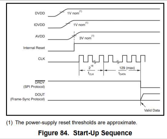
- Star-Up Sequence
. At power-on, bring up the DVDD supply first, followed by IOVDD and then AVDD. Check the first, followed by IOVDD and then AVDD. Check the power-supply sequence for proper order, including the ramp rate of each supply. DVDD and IOVDD may be sequenced at the same time (for example, if the supplies are tied together). Each supply has an internal reset circuit whose outputs are summed together to generate a global power-on reset. After the supplies have exceeded the reset thresholds, 2^18 fCLK cycles are counted before the converter initiates the conversion process. Following the CLK cycles the data for 129 conversions are suppressed by the ADS1274/78 to allow output of fully-settled data.
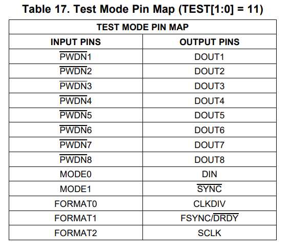
- Test Pin
|
[TEST1:TEST0] |
TEST Mode |
|
00 |
Normal operation |
|
01 |
Reserved |
|
10 |
Reserved |
|
11 |
Test Mode |
- 1278 竞品测试结果
- 1278电路设计
8.1)AGND和DGND可以使用同一个人地平面
8.2)数字输入脚需要串接50欧电阻,并放置在数字驱动源末端(靠近1278)
8.3)模拟电路(输入脚)走线必须远离数字电路(输入脚)并防止产生走线交叉
84.)模拟信号参考端接10uF和0.1uF电容
今天的文章ADS1278学习总结分享到此就结束了,感谢您的阅读,如果确实帮到您,您可以动动手指转发给其他人。
版权声明:本文内容由互联网用户自发贡献,该文观点仅代表作者本人。本站仅提供信息存储空间服务,不拥有所有权,不承担相关法律责任。如发现本站有涉嫌侵权/违法违规的内容, 请发送邮件至 举报,一经查实,本站将立刻删除。
如需转载请保留出处:https://bianchenghao.cn/33569.html

